Atomic-layer-deposited silicon-nitride/SiO2 stacked gate dielectrics for highly reliable p-metal–oxide–semiconductor field-effect transistors
Applied Physics Letters Volume 77 Issue 18
Page 2855-2857
published_at 2000-10-30
アクセス数 : 1136 件
ダウンロード数 : 255 件
今月のアクセス数 : 0 件
今月のダウンロード数 : 0 件
この文献の参照には次のURLをご利用ください : https://ir.lib.hiroshima-u.ac.jp/00018596
| File | |
| Title ( eng ) |
Atomic-layer-deposited silicon-nitride/SiO2 stacked gate dielectrics for highly reliable p-metal–oxide–semiconductor field-effect transistors
|
| Creator |
Yoshimoto Takashi
Kidera Toshiro
Obata Katsunori
Sunami Hideo
Hirose Masataka
|
| Source Title |
Applied Physics Letters
|
| Volume | 77 |
| Issue | 18 |
| Start Page | 2855 |
| End Page | 2857 |
| Abstract |
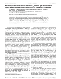
An extremely thin (~0.4 nm) silicon-nitride layer has been deposited on thermally grown SiO2 by an atomic-layer-deposition (ALD) technique. The boron penetration through the stacked gate dielectrics has dramatically been suppressed, and the reliability has been significantly improved, as confirmed by capacitance–voltage, gate-current–gate-voltage, and time-dependent dielectricbreakdown characteristics. The ALD technique allows us to fabricate an extremely thin, very uniform silicon-nitride layer with atomic-scale control.
|
| Language |
eng
|
| Resource Type | journal article |
| Publisher |
American Institute of Physics
|
| Date of Issued | 2000-10-30 |
| Rights |
Copyright (c) 2000 American Institute of Physics.
|
| Publish Type | Version of Record |
| Access Rights | open access |
| Source Identifier |
[ISSN] 0003-6951
[DOI] 10.1063/1.1320847
[NCID] AA00543431
[DOI] http://dx.doi.org/10.1063/1.1320847
|


